1 Wuhan National Laboratory for Optoelectronics, Huazhong University of Science and Technology, Wuhan 430074, China
2 State Key Laboratory of Advanced Optical Communication Systems and Networks, School of Electronics, Peking University, Beijing 100871, China
In the past half century, silicon-based microelectronics and optical fiber communication have triggered a far-reaching information technology revolution, which has moved human society into a high-speed information age. The demand for communication capacity and speed is growing exponentially. On the other hand, data center and high-performance computing are facing bottlenecks of speed, bandwidth, and energy consumption of electrical interconnections. Siliconbased optoelectronics has become the key technology to break through these bottlenecks. Thanks to the advantages of high refractive index, capable in small active components, and CMOS compatible process, silicon can achieve a largescale optoelectronic integration on a micro-chip with low cost and low energy consumption. This has become a hot alternative for the chip industry. In addition, silicon-based optoelectronics has enabled a series of new study fields such as mid-infrared communication, microwave optoelectronics, lab-on-chip, quantum communication, optoelectronic computing, and chip scale lidar.
Frontiers of Optoelectronics
2022, 15(2): s12200

Author Affiliations
Abstract
1 Peking University, State Key Laboratory of Advanced Optical Communication Systems and Networks, School of Electronics, Beijing, China
2 Chinese Academy of Sciences, Shanghai Institute of Optics and Fine Mechanics, Shanghai, China
Conventional electronic processors, which are the mainstream and almost invincible hardware for computation, are approaching their limits in both computational power and energy efficiency, especially in large-scale matrix computation. By combining electronic, photonic, and optoelectronic devices and circuits together, silicon-based optoelectronic matrix computation has been demonstrating great capabilities and feasibilities. Matrix computation is one of the few general-purpose computations that have the potential to exceed the computation performance of digital logic circuits in energy efficiency, computational power, and latency. Moreover, electronic processors also suffer from the tremendous energy consumption of the digital transceiver circuits during high-capacity data interconnections. We review the recent progress in photonic matrix computation, including matrix-vector multiplication, convolution, and multiply–accumulate operations in artificial neural networks, quantum information processing, combinatorial optimization, and compressed sensing, with particular attention paid to energy consumption. We also summarize the advantages of silicon-based optoelectronic matrix computation in data interconnections and photonic-electronic integration over conventional optical computing processors. Looking toward the future of silicon-based optoelectronic matrix computations, we believe that silicon-based optoelectronics is a promising and comprehensive platform for disruptively improving general-purpose matrix computation performance in the post-Moore’s law era.
silicon-based optoelectronics photonic matrix computation optical interconnections photonic-electronic integration Advanced Photonics
2022, 4(4): 044001

Author Affiliations
Abstract
1 State Key Laboratory of Advanced Optical Communication Systems and Networks, Department of Electronics, School of Electronics Engineering and Computer Science, Peking University, Beijing 100871, China
2 Guangxi Key Laboratory of Precision Navigation Technology and Application, Guilin University of Electronic Technology, Guilin 541004, China
3 Shanghai Institute of Optics and Fine Mechanics, Chinese Academy of Sciences, Shanghai 201800, China
Nano-focusing structures based on hybrid plasmonic waveguides are likely to play a key role in strong nonlinear optical devices. Although the insertion loss is considerable, a significant nonlinear phase shift may be achieved by decreasing the nano-focusing device footprint and careful parameter optimization. Here, we study the Kerr effect in hybrid plasmonic waveguides by analyzing the mode effective area, energy velocity, and insertion loss. Particularly, by utilizing plasmonics to manipulate the effective index and mode similarity, the TM mode is reflected and absorbed, while the TE mode passes through with relatively low propagation loss. By providing a deep understanding of hybrid plasmonic waveguides for nonlinear applications, we indicate pathways for their future optimization.
silicon photonics plasmonics nonlinear optics nano-focusing Chinese Optics Letters
2022, 20(3): 031903
1 江南大学物联网工程学院,江苏 无锡 214122
2 江南大学物联网技术应用教育部工程研究中心,江苏 无锡 214122
在增强现实领域,实现虚拟对象光照一致性一直是个难题,针对赋予虚拟对象阴影信息时阴影检测效率低的问题,提出一种基于阴影区域构建阴影体实现虚拟对象光照一致性的方法。首先,采用改进的超像素分割(Ⅰ-SLIC)算法对图像进行处理得到更稳定的超像素集合,并根据相邻超像素中心的颜色距离相似度进行超像素合并,以降低后续处理复杂度。然后,采用高斯混合背景模型对分割后的图像进行阴影检测,利用阴影区域与光照参数构建阴影体。最后,根据变换矩阵完成虚拟对象的注册并结合阴影体进行渲染。实验结果表明,所提方法实现了对虚拟对象的阴影渲染,大大提高了增强现实应用带来的真实感,对比其他方法,在时间效率上具有明显优势。
机器视觉 增强现实 光照一致性 阴影检测 超像素分割 激光与光电子学进展
2022, 59(2): 0215002

Author Affiliations
Abstract
1 State Key Laboratory of Advanced Optical Communication Systems and Networks, Department of Electronics, School of Electronics Engineering and Computer Science, Peking University, Beijing 100871, China
2 Peking University Shenzhen Research Institute, Shenzhen 518057, China
3 Nano-optoelectronics Frontier Center of Ministry of Education, Peking University, Beijing 100871, China
A low-loss hybrid plasmonic transverse magnetic (TM)-pass polarizer has been demonstrated utilizing polarization-dependent mode conversion. Taking advantage of the silicon hybrid plasmonic slot waveguide (HPSW), the unwanted transverse electric (TE) fundamental mode can be efficiently converted first to a TM higher-order mode and then suppressed by a power combiner, while the retained TM fundamental mode can pass through with negligible influence. Since the HPSW feature both strong structural asymmetry and a small interaction area in the cross-section between the metal and optical field, the optimized insertion loss of the device is as low as 0.4 dB. At the wavelength of 1550 nm, the extinction ratio is 28.3 dB with a moderate footprint of . For the entire C band, the average reflection of the TE mode is suppressed below , and the extinction ratio is over 18.6 dB. This work provides another more efficient and effective approach for better on-chip polarizers.
Photonics Research
2020, 8(7): 07001197
1 北京大学信息科学技术学院电子系区域光纤通信网与新型光通信系统国家重点实验室, 北京 100871
2 北京大学深圳研究院, 广东 深圳 518057
3 北京大学纳光电子前沿科学中心, 北京 100871
4 华为技术有限公司中央研究院数据中心技术实验室, 广东 深圳 518000
数十年来,人们一直在探索基于光的计算体系,期望通过光的特性,突破电子计算机的局限,从而提高计算速度和降低能耗。然而,传统光计算由于缺乏有效的逻辑、存储、互连单元,以及合理的应用场景,光计算止步于概念研究阶段。在当今大数据时代的推动下,信息通量及用量呈爆炸性增长。具有高集成度、大带宽、低成本、低能耗特征的硅基光电子技术应运而生,日趋成熟,并且验证了光电融合这一信息技术发展的趋势。光计算也随之向光电计算转变。分析近年来硅基光电子技术在光电计算方面的应用和发展,如在人工神经网络、非多项式时间复杂度难题的启发式算法、光电模拟计算、集成光电量子处理器和神经拟态计算等,重点论述了硅基光电子技术在促进光电计算的信息连接、数据处理和实用化演进等方面的优势,提出了硅基光电计算概念及初级系统,以突破传统电子技术或光子技术在计算方面的不足及其在人工智能等高性能计算领域中的限制。
光计算 硅基光电子 硅基光电计算 硅光人工智能 光电人工神经网络 硅光模拟计算

Author Affiliations
Abstract
1 State Key Laboratory of Advanced Optical Communication Systems and Networks, School of Electronics Engineering and Computer Science, Peking University, Beijing 100871, China
2 Peking University Shenzhen Research Institute, Shenzhen 518057, China
3 Nano-optoelectronics Frontier Center of Ministry of Education, Peking University, Beijing 100871, China
Optical microring resonators are extensively employed in a wide range of physical studies and applications due to the resonance enhancement property. Incorporating coupling control of a microring resonator is necessary in many scenarios, but modifications are essentially added to the resonator and impair the capability of optical enhancement. Here, we propose a flexible coupling structure based on adiabatic elimination that allows low-loss active coupling control without any modifications to the resonators. The self-coupling coefficient can be monotonically or non-monotonically controllable by the proposed coupler, potentially at a high speed. The characteristic of the coupler when implemented in silicon microring resonators is investigated in detail using substantiated analytical theory and experiments. This work provides a general method in coupling control while ensuring the resonance enhancement property, making active coupling control in a resonator-waveguide system feasible.
silicon photonics adiabatic elimination resonance system Chinese Optics Letters
2020, 18(1): 013601
1 江南大学物联网工程学院, 江苏 无锡 214122
2 江南大学物联网技术应用教育部工程研究中心, 江苏 无锡 214122
针对增强现实中基于目标点云的跟踪与注册问题,提出一种稳健Z分数混合树的配准算法。通过局部邻域内的点至拟合平面的垂直距离以及沿平面法线点的分布来识别噪点,运用绝对中位差增强Z分数的稳健性,同时,采用混合树算法提高最近点的搜索效率。将上述算法应用于增强现实的成像原理中,以对其进行理论论证。分别利用斯坦福大学某研究组的点云数据集和真实采集数据对该算法进行验证。结果表明,在含噪点云集中,该算法能在保持一定精度的同时有效提高配准效率,其用时约为对比算法的5%~10%。
图像处理 点云配准 增强现实 Z分数 模糊近邻 激光与光电子学进展
2019, 56(19): 192803
1 江南大学物联网工程学院, 江苏 无锡 214122
2 江南大学物联网技术应用教育部工程研究中心, 江苏 无锡 214122
在无标记增强现实中,基于视觉即时定位与地图构建,结合ORB特征提取算法和顺序抽样一致性,提出了一种改进的注册方法。利用相似函数衡量匹配样本点对之间的差异性,从具有最高品质函数的数据子集中抽取样本,得到较优的匹配点对,完成了三维地图重建过程中的平面检测。通过奇异值分解,实现了虚拟物体的方向和位置控制;结合相机的位姿估计,完成了虚拟物体的注册。实验结果表明,所提方法的平均注册效率提高了34.5%。
机器视觉 增强现实 注册 视觉即时定位与地图构建 顺序抽样 ORB算法 激光与光电子学进展
2019, 56(6): 061501
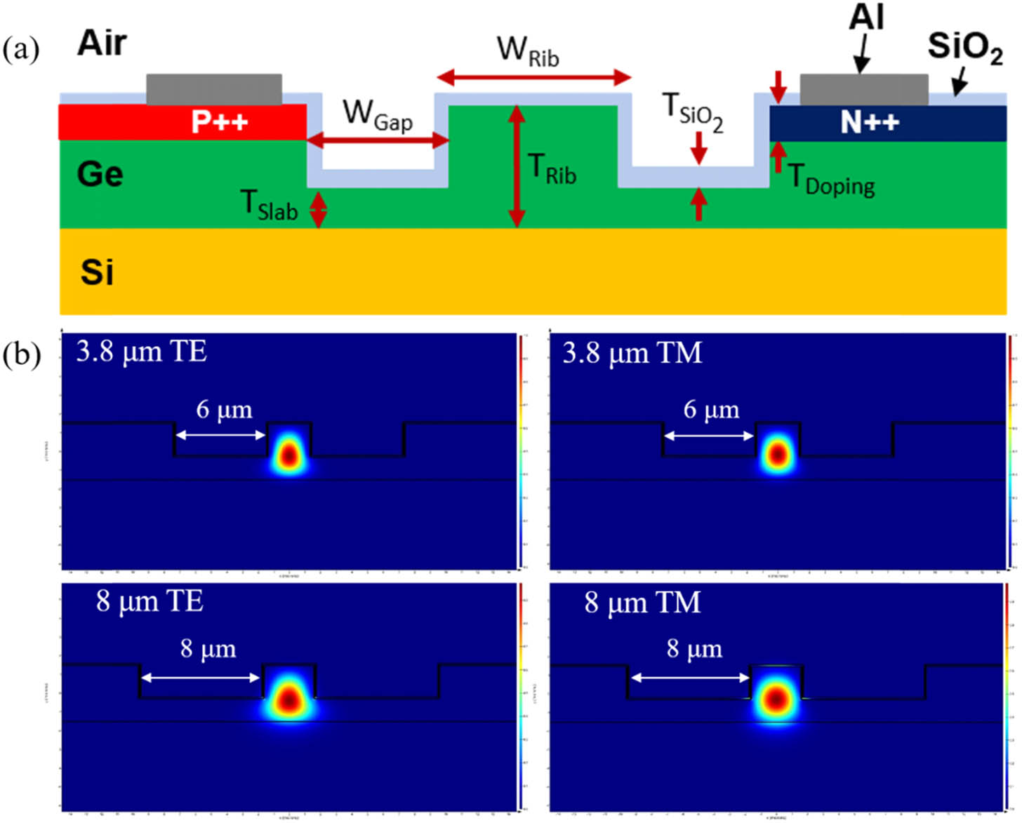
Author Affiliations
Abstract
1 Optoelectronics Research Centre, University of Southampton, Southampton SO17 1BJ, UK
2 State Key Laboratory of Advanced Optical Communication Systems and Networks, School of Electronics Engineering and Computer Science, Peking University, Beijing 100871, China
3 Silicon Technologies Centre of Excellence, Nanyang Technological University, Singapore 639798, Singapore
4 Centre de Nanosciences et de Nanotechnologies, CNRS, Univ. Paris-Sud, Université Paris-Saclay, C2N—Palaiseau, 91120 Palaiseau, France
We report mid-infrared Ge-on-Si waveguide-based PIN diode modulators operating at wavelengths of 3.8 and 8 μm. Fabricated 1-mm-long electro-absorption devices exhibit a modulation depth of >35 dB with a 7 V forward bias at 3.8 μm, and a similar 1-mm-long Mach–Zehnder modulator has a Vπ·L of 0.47 V·cm. Driven by a 2.5Vpp RF signal, 60 MHz on-off keying modulation was demonstrated. Electro-absorption modulation at 8 μm was demonstrated preliminarily, with the device performance limited by large contact separation and high contact resistance.
Photonics Research
2019, 7(8): 08000828


